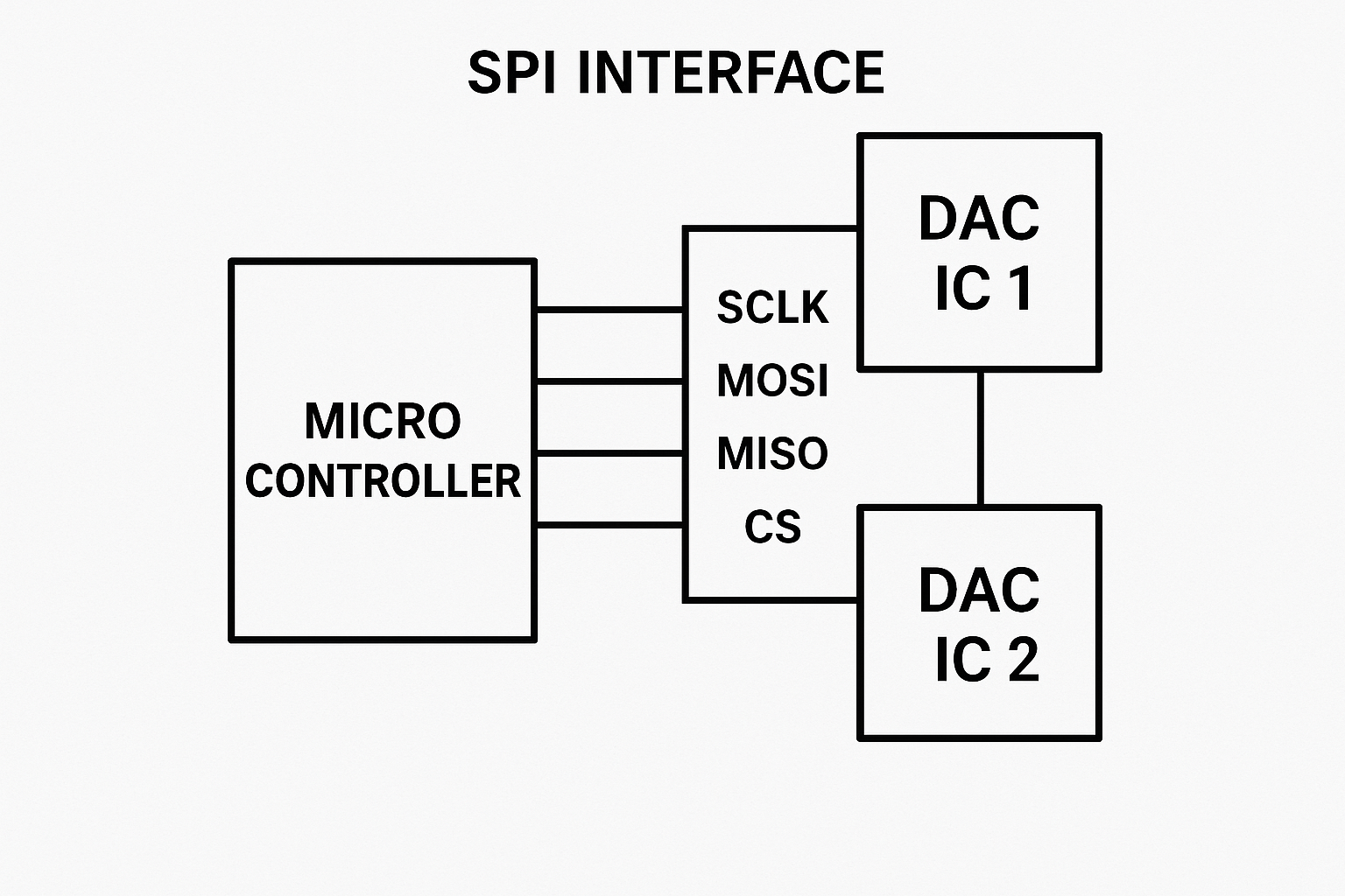
Digital-to-Analog Converters (DACs) play a major role in the embedded systems by translating digital values into analog voltages. To interface the DAC8551 (TI) using SPI on a TI microcontroller platform, leveraging TI’s driver libraries for clean and modular code.
It can be used to modulate the output voltage via a program through the SPI interface by writing to the ADC registers: write 0x0000 to produce the minimum voltage and 0xFFFF to produce the maximum voltage.
Overview
The DAC8551 is a high-resolution, 16-bit single-channel DAC that communicates over SPI. It expects a 24-bit command frame:
[6 unused bits ][2 power-down bits ][16-bit DAC value ]

We will use the TI’s TI-RTOS (or equivalent driver framework) to:
* Initialize the SPI peripheral
* Construct and transmit command frames to the DAC
* Gradually change DAC output using pre-defined percentages

📁 Project Setup
Make sure you are configured your project in TI CCS (Code Composer Studio) and Enable the SPI (CONFIG_SPI_0).
Steps:
* Open CCS and import the (SPI peripheral) example from resource explorer
* Open Sysconfig and Add SPI with name of (CONFIG_SPI_0)
* Select Four Pin CS Active Low mode and Config all the Pins for SPI In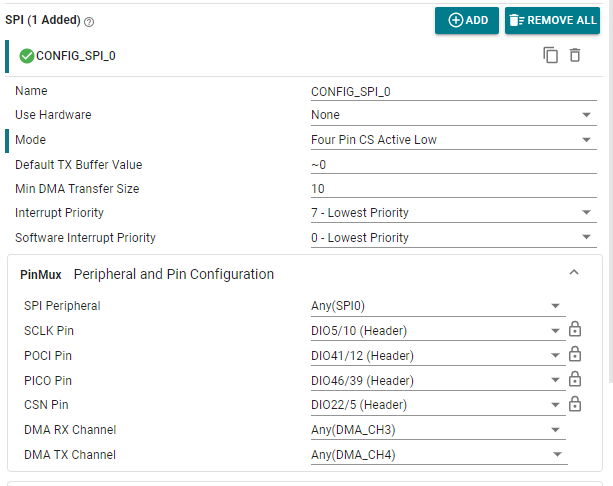
SCLK = CLK
POCI = MOSI
PICO = MISO
CSN = CS
The DAC8551 IC does not have a MISO pin, It is a unidirectional (one-way) device. Therefore, a dummy pin can be assigned for MISO to satisfy the SPI interface requirements.
📦 Header files
#include <stdint.h>
#include <stdbool.h>
#include <ti/drivers/SPI.h>
#include <ti/drivers/GPIO.h>
#include <ti/drivers/dpl/ClockP.h>
#include "ti_drivers_config.h"
These headers bring in fixed-width integer types, SPI/GPIO functionality, and timing functions (ClockP_sleep, ClockP_usleep).
Initializing the SPI for DAC8551
static SPI_Handle dacSpi;

void DAC8551_init(void)
{
    SPI_Params spiParams;
    SPI_Params_init(&spiParams);

    spiParams.frameFormat = SPI_POL0_PHA1;  // SPI Mode 1
    spiParams.dataSize    = 8;              // 8-bit data frames
    spiParams.bitRate     = 1000000;        // 1 MHz

    dacSpi = SPI_open(CONFIG_SPI_0, &spiParams);
    if (dacSpi == NULL) {
        while (1) { /* SPI init failed */ }
    }
}- Open SPI port
CONFIG_SPI_0in Mode 1 (CPOL = 0,CPHA = 1). dataSize = 8which means SPI will transmit 3 separate bytes to send the required 24 bits.- A safe 1 MHz clock rate is used for compatibility with the DAC8551 clock timing spec.
📤 Writing Register to the DAC IC
bool DAC8551_writeRegister(uint16_t value, uint8_t pd)
{
    SPI_Transaction trans;
    uint8_t txBuf[3];

    uint32_t frame = ((uint32_t)(pd & 0x03) << 16) | (uint32_t)value;

    txBuf[0] = (uint8_t)((frame >> 16) & 0xFF);
    txBuf[1] = (uint8_t)((frame >> 8) & 0xFF);
    txBuf[2] = (uint8_t)(frame & 0xFF);

    trans.count = 3;
    trans.txBuf = txBuf;
    trans.rxBuf = NULL;

    return SPI_transfer(dacSpi, &trans);
}- Constructs a 24-bit command frame:
- Top 6 bits: unused (zeros)
- Next 2 bits:
pd(power-down control, usually 0 for normal mode) - Final 16 bits: DAC value (0 to 65535)
- Transmits the frame as 3 bytes over SPI Interface.
Main: Stepping Through Output Levels
void *mainThread(void *arg0)
{
    SPI_init();
    GPIO_init();
    DAC8551_init();

    const int percents[] = {10, 40, 60, 100};
    const int nSteps = sizeof(percents) / sizeof(percents[0]);
    const int delay_ms = 20000; // 20 seconds
    const uint32_t FULL = 65535U;

    while (1) {
        for (int i = 0; i < nSteps; ++i) {
            uint32_t p = (uint32_t)percents[i];

            uint32_t code = (p * FULL + 50U) / 100U;
            if (code > FULL) code = FULL;

            DAC8551_writeRegister((uint16_t)code, 0); // pd = 0 (normal)
            ClockP_sleep(delay_ms / 1000);
            ClockP_usleep((delay_ms % 1000) * 1000);
        }
    }
}
📈 What This Does:
- Initializes peripherals.
- Define the target DAC output as a percentage if a fixed output level is needed. You can specify the desired percentage directly or alternatively, write the corresponding DAC code value using a function call like
DAC8551_writeRegister(0xFFFF, 0)instead of using a for-loop. - Converts each percentage to a 16-bit DAC code using:
code = (p * 65535 + 50) / 100This avoids floating-point math and ensures the percentage value rounding is correct. - Sends the value to DAC.
- Waits 20 seconds between the each change using
ClockP_sleep()andClockP_usleep(). - The waiting time after a voltage change is used to verify the stability of the output voltage and to measure the test duration.
How the Output Works
If your DAC reference voltage (Vref) is 0 to 3.3V, the output voltages will be approximately:
| Percent | DAC Code | Output Voltage |
|---|---|---|
| 10% | 6554 | ~0.33V |
| 40% | 26214 | ~1.32V |
| 60% | 39321 | ~1.98V |
| 100% | 65535 | ~3.3V |
These values will repeat in a loop, with 20-second intervals between each change we made.
This approach is useful for most DAC applications for variable outputs including waveform generation, sensor simulation, 0 to 10v Conversion, or analog control systems.